A roadmap to meet the demand for silicon photonics fabrication in the UK
Callum Littlejohns is the coordinator of the CORNERSTONE programme, a silicon photonics rapid prototyping fabrication service based at the University of Southampton. He shares his insights into the current UK silicon photonics research space and the direction it may take over the next decade.
How high is the current demand for silicon photonics?
Silicon photonics technology uses silicon as a platform for photonic circuits to create the next generation of highly integrated optical communication systems and data infrastructure. Silicon photonics is a market that exceeded $600 million in 2019 and is poised to grow at over 30 per cent CAGR between 2020 and 2026. The need of silicon photonics in data centre application areas will continue to drive the market forward.
But it is not just about bandwidth anymore. For example, integrated silicon photonics has the ability to fundamentally change some notions of computing, it is also making its way into consumer devices such as medical sensors in smart watches. The industry is just beginning to see what may be possible, but it will need to adapt to meet the demands being placed on it and solve the bottlenecks in the design, development and fabrication of integrated silicon photonics.
How is CORNERSTONE helping to meet the demand for silicon photonics?
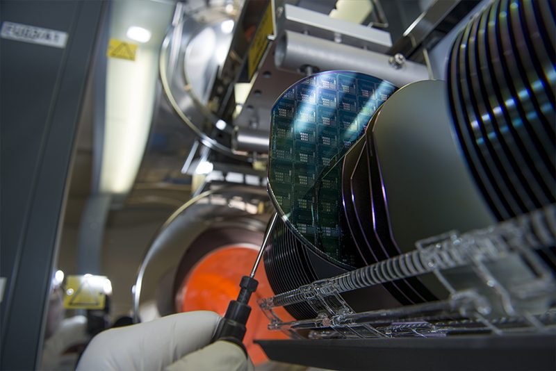
We launched CORNERSTONE in 2017 through an ESPRC grant. It is a rapid prototyping fabrication facility that produces silicon photonics devices on large eight inch wafers, resulting in a much bigger throughput than a typical university facility, at a cost-effective level. The technology platform utilises industrially-compatible tools such as deep-UV projection lithography, to enable seamless scaling-up of production volumes. We follow the tried and tested multi-project-wafer (MPW) approach whereby our users are able to purchase a small area of the wafer for their design to be built on. This cost sharing mechanism has been very successful in opening up the technology to researchers who do not have their own facility or technology to prototype silicon photonics devices. Where CORNERSTONE differentiates itself from other foundries is the flexibility it offers in its fabrication processes that supports innovation at the device level. Our users are able to access CORNERSTONE to prototype their devices in the development phase, at a cost-effective level, before transferring to larger foundries that specialise in mass production.
What new platforms are you working on?
CORNERSTONE has been a really successful addition to the UK photonics landscape. We’ve had 43 different research groups use our capability from 15 different countries, but now our users are telling us they want more – and we are listening. We’re looking at using different materials to support emerging applications, not just silicon, and these will be launched later this year. The first is silicon nitride. The benefit of this platform is less power is lost when light is guided through it and it also supports different wavelengths. It supports visible wavelengths, which is important for quantum computing and more. The second platform is suspended silicon, which supports longer wavelengths and the third is germanium on silicon, and that extends the transparency even further. These platforms are important for sensing applications, where different chemical or biological compounds will absorb light of a specific wavelength. In addition, we are introducing electronics integration platforms to further increase the functionality of silicon photonics integrated circuits and exploring means of integrating light sources onto the same chip – a major challenge for silicon photonics. Our research group has been working with these platforms for a while now and know there’s a demand for it to be scaled up and we hope that it will give researchers numerous options when designing optoelectronics devices and systems.
How can the Hub support this work?
CORNERSTONE has been very successful in reducing the barriers to entry, particular for smaller companies and researchers without big budgets or their own facilities. The Hub supports this work by taking it one step further and linking it to industry and mass production and we are lucky that CORNERSTONE’s Principal Investigator is Professor Graham Reed who is also a Co-Investigator in the Hub. The commercialisation process is something that is perhaps lacking – we are excellent at doing research but the business and enterprise side of it needs to be developed, which is where support from programmes like the Hub, can really help.
Where do you see silicon photonics research developing over the next five to ten years?
There are two major areas which will rapidly expand over the next decade and these are sensing and LiDAR.
Sensing could be the biggest thing for silicon photonics. Technology is being built to enable a clinic on a wrist and there are lots of medical sensing companies emerging based on silicon photonics technology. Another sensing application is monitoring of greenhouse gas emissions from the ocean, where current large fragile systems on ships have high carbon footprints. Silicon photonics sensing technologies will transform measurement of the impact of climate change mitigation strategies.
LiDAR is a method for determining variable distances with high accuracy using light-based technologies including silicon photonics. It can be used in applications for driverless cars and drones.
The consumer markets in both of these areas are going to make them take off and that’s really the selling point of silicon photonics – the materials you use are the same as electronics. Silicon itself may not be the best material optically, but its cost and scalability of processing makes it very attractive and accessible. This is demonstrated by the fact that some of big electronics foundries like TSMC, are getting involved in silicon photonics.